Design
I needed a MOSFET Shield for a Wemos D1 mini to drive solenoids and relays. I could not find anything suitable online, so I decided to design and build my own. The board size of a Wemos D1 mini is quite small (1″ x 1.3″) and part of that is the PCB antenna, so a shield should avoid covering the area over the antenna with copper or lots of components.

Wemos D1 Mini ESP8266 Development Board
I wanted the shield to be the same size as the Wemos D1 mini. I need to be able to switch about 12v at about 2A. Most use cases I had were small relays and solenoids.
I found a very small dual channel MOSFET in a 2mm x 2mm package (FDMA1024NZ – Dual N-Channel MOSFET 20V / 5.0A). This MOSFET is so small I could fit two on the shield, giving a total of four channels.

Wemos D1 Mini MOSFET Shield 4ch v1.3 Schematic

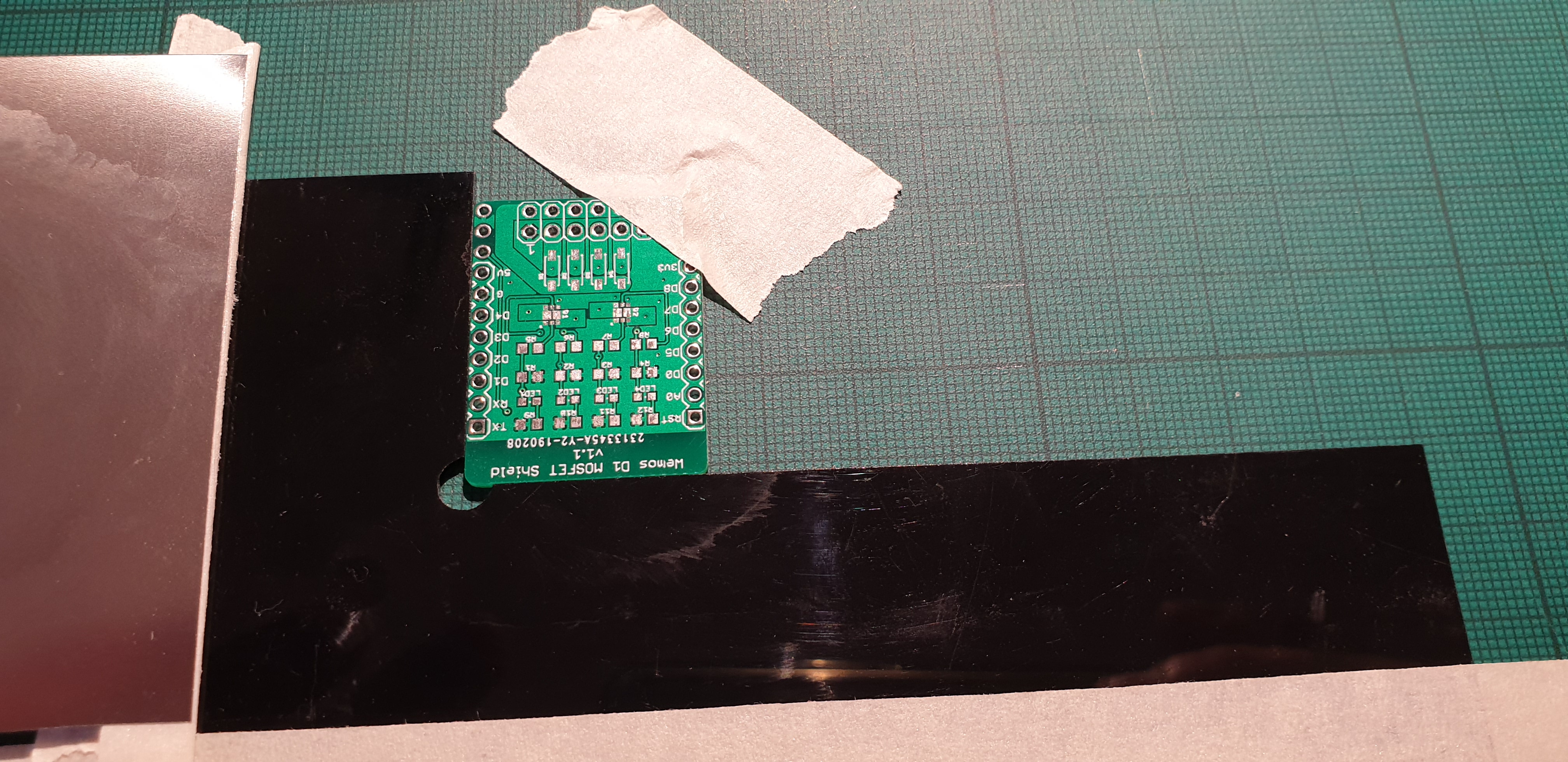
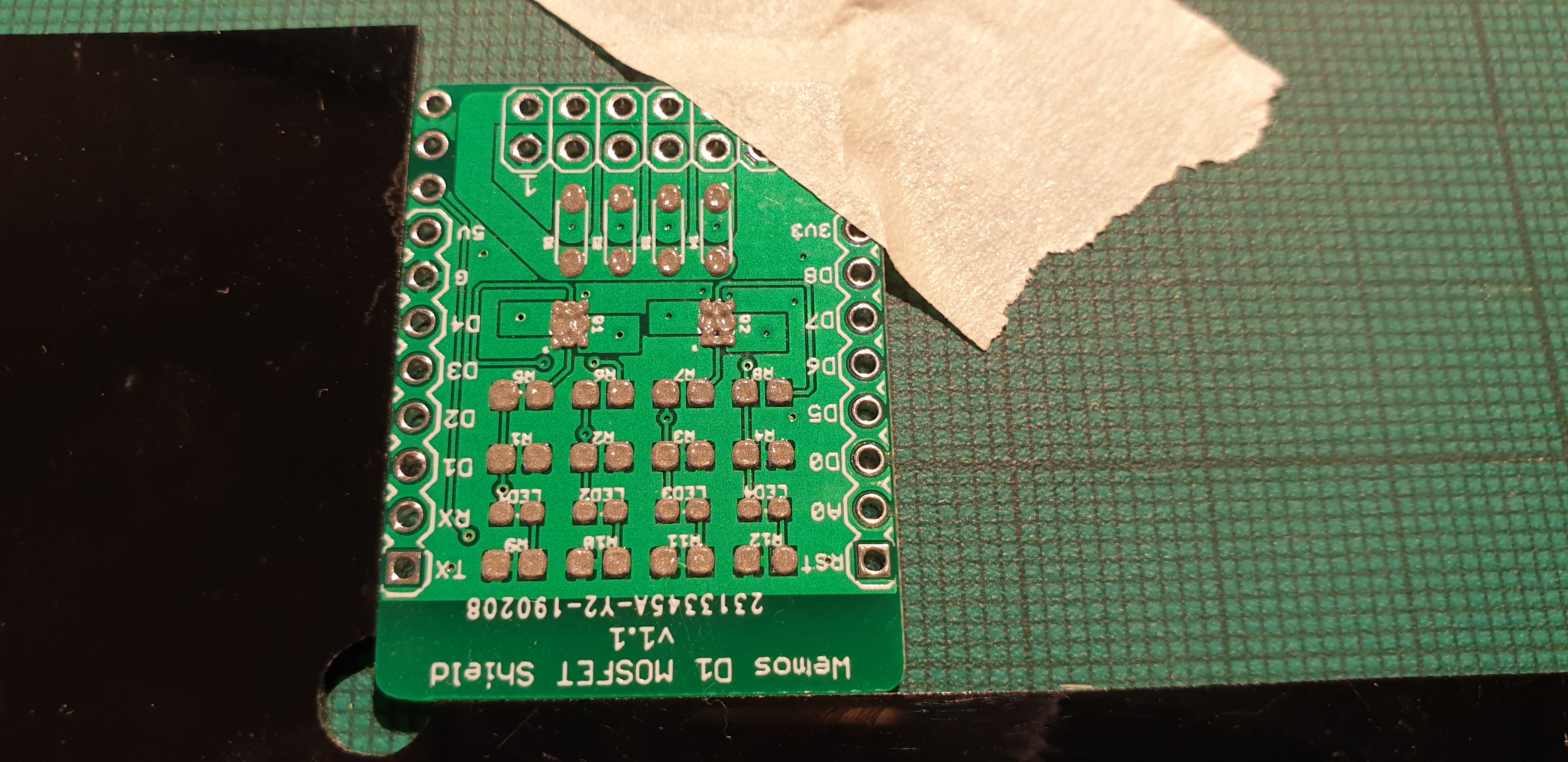
Wemos D1 Mini MOSFET Shield 4ch v1.1 Board
Fabrication
I created the board design and ordered the PCBs and a solder stencil for the first prototype. The 2mm x 2mm package is very difficult, if not impossible, to hand solder, so the stencil would allow me to stencil the solder paste and hand place the components, before reflowing it in an oven.
Before solder stencilling

During solder stencilling
After solder stencilling

Close up of solder stencilling and component placement

First prototype completed
The first version worked perfectly, but the 2mm x 2mm MOSFET was a little obscure and difficult to hand solder. In addition, JLC PCB had launched a pick and place PCB fabrication service which was very economical. I thought I’d try it for my MOSFET board, but the MOSFETs I was using were not supported. So I replaced the two obscure dual MOSFETs with four discrete MOSFETs which JLC support as a basic components.

Wemos D1 Mini MOSFET Shield 4ch v1.3 Board
The JLC PCB fabrication service built a batch which again all worked perfectly.
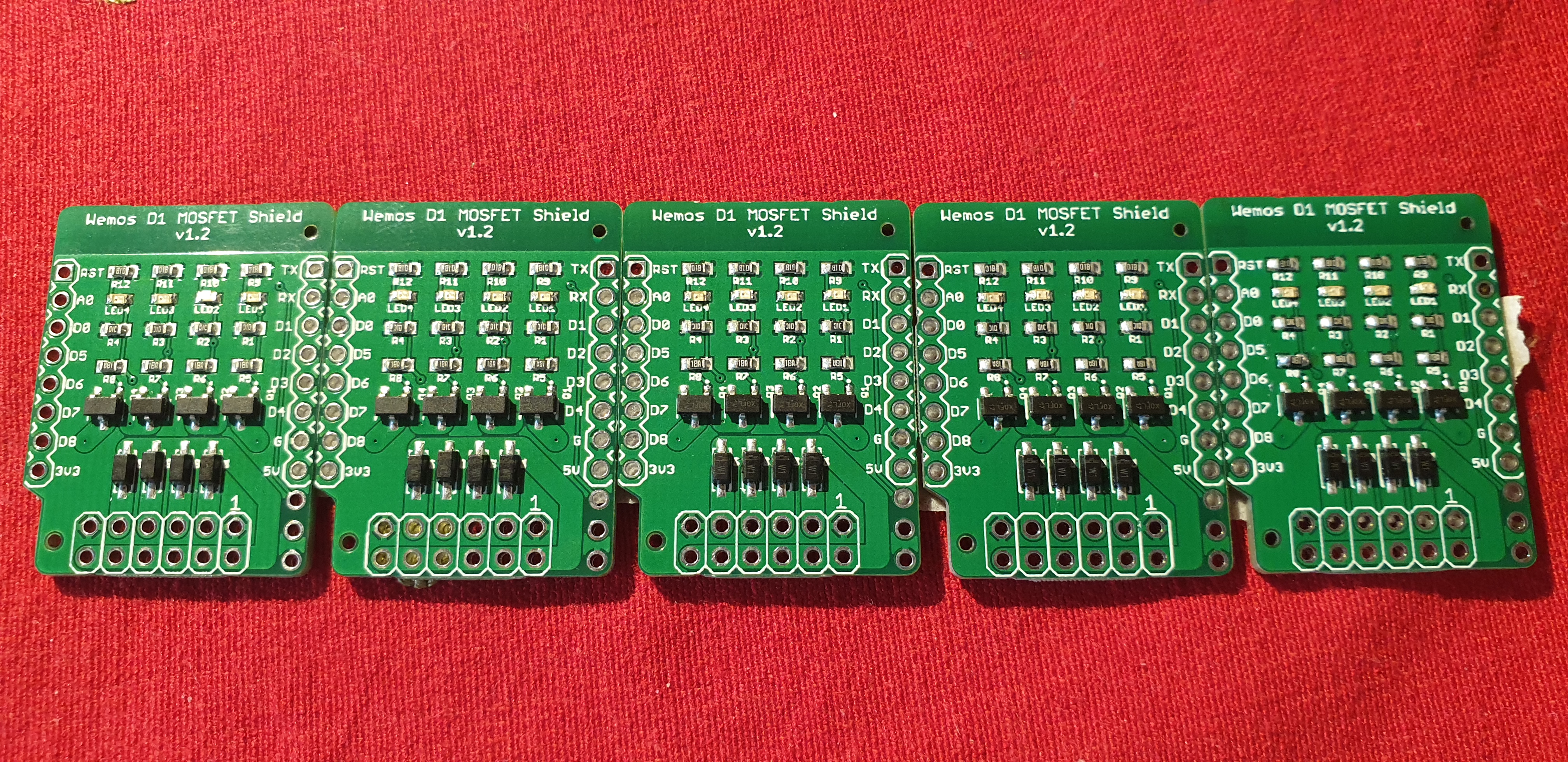
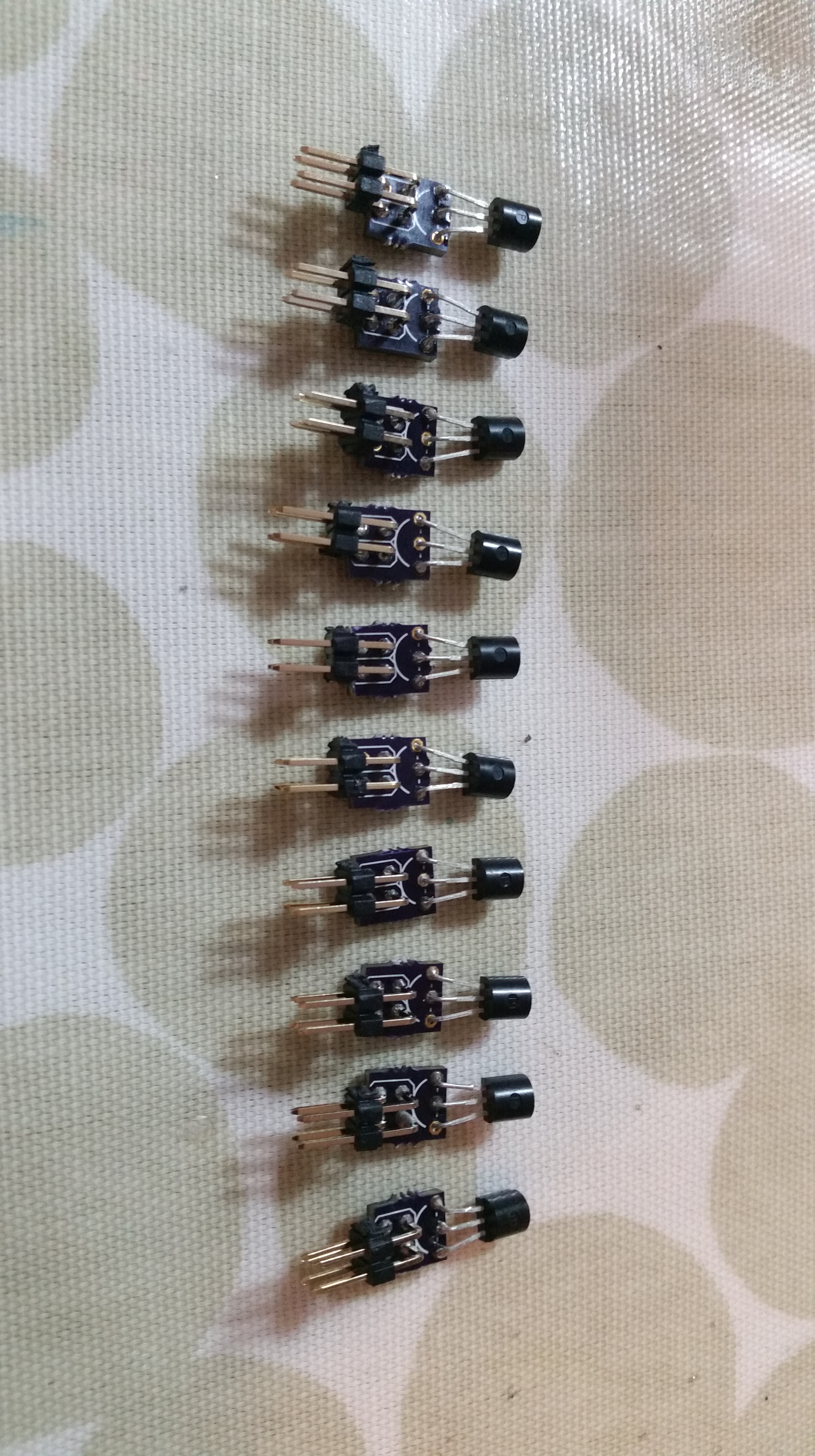
MOSFET Shields for Wemos D1 Mini v1.2
Testing
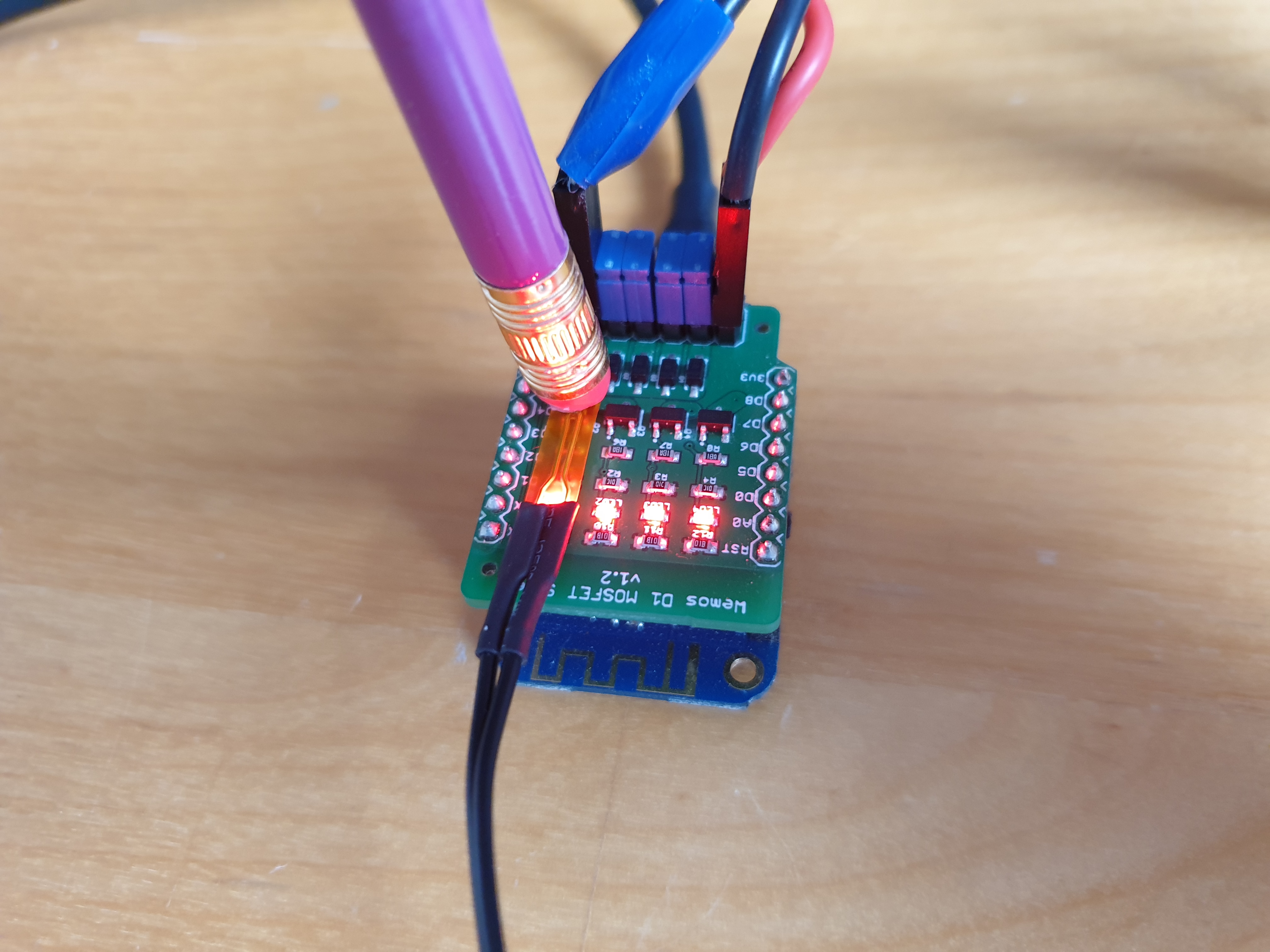
I needed to test the board design to ensure it could handle the current rating. The MOSFETs are rated at a maximum of 5A each. So, each individual channel should switch 5A. In addition all four channels can be connected together which would switch about 20A in total. I wanted to make sure the tiny PCB would handle this load. I designed the power traces on the PCB to be as wide as the physical dimensions of the board would allow.
I bought a 180W battery tester from BangGood to use as a variable load which could test up to 20A and 180W. This device has lots of useful features. You can configure it as a constant current load in 10mA increments. It measures voltage, current, power and even temperature using a plug in thermocouple, and displays all the readings in real time on a colour LCD. Its a very functional device for a very economical price.
To source 20A, I decided to use a lead acid battery. I don’t have a bench power supply that can easily provide 20A. I used thick 12AWG wire to connect the battery to the variable load and the shield under test.

MOSFET Shield for Wemos D1 mini Power Testing Setup
The test setup consisted of;
- A 12v lead acid battery
- The variable load
- The shield under test – with the MOSFET outputs shorted together

Power Testing Setup
I planned to test each individual channel at 1A, 2A, 3A, 4A & 5A, while monitoring the temperature of the MOSFET, PCB traces and connectors. In addition, I want to connect all four channels together and test up to 20A.
The first few tests went well. Each channel can handle up to 5A. The MOSFETs get a little warm at 5A. If the board is used at maximum capacity for long periods, it would benefit from either forced air cooling or a small heat sink on the MOSFETs.
MOSFET Shield for Wemos D1 mini Power Testing Temperature
I struggled to test all channels to a total of 20A. The battery tester I had can only handle 180W, and the only convenient 20A source I had was a 12v lead acid battery. 12v @ 20A is 240W which is more than 180W, and the tester cuts out when it hits 180W.
I managed to test up to 16A with the lead acid battery setup, which was right on the limit of the 180W limit.

MOSFET Shield for Wemos D1 mini Power Testing 16A
I had a small 2S LiPo at 7.2v and managed to complete a final test of 20A using this LiPo, but at 20A is the battery discharged very quickly and the voltage would drop to 6v very quickly and the tester cuts out at 6v to protect the battery from over discharge.

MOSFET Shield for Wemos D1 mini Power Testing 18A
I’m confident the boards will operate to 5A per channel, to a maximum combined current of 18A as I managed to successfully test to both these levels. At higher currents the individual MOSFETs get hot and the Dupont header does. I think the header pins are only rated to 5A, so for 20A the board would need a redesign with more power pins to distribute the load. 4A per channel is way more than most of my projects need, so I’m happy with the design. If you really need to switch 20A for short periods of time, use a heatsink and solder the wires directly to the board rather than use pin headers and a Dupont connector.
Batch production
The shields were used in three of my home automation projects:
- Automatic Garden Watering to control four water solenoids connected to garden hoses.
- Immersion Heater Controller to control 2 high current relays to switch two 3kW hot water immersion heaters.
- Automatic plant Pot Watering to control a small peristaltic pump to water pot plants based on moisture reading from a capacitive moisture sensor. This was the project that I added the analogue in header on the shield for. This allowed me to connect the moisture sensor and the peristaltic pump to the same shield.
Once the shields had been running in projects for a couple of months, without any issues, I decided to build a small batch to sell online. If I couldn’t find something similar online, then maybe others would like to buy these to use in their robotics or home automation projects.

MOSFET Shield for Wemos D1 mini v1.3 Panel for Fabrication
The four channel MOSFET shield can be purchased here on Tindie.

Final Specification
- Dimensions : 1″ x 1.3″ x 0.063″ (25.4mm x 33.0 x 1.6mm)
- Four MOSFETs : AO3400A – 30V N-Channel
- Maximum Drain-Source Voltage : 30v
- Continuous Drain Current : 5A
- GPIO pins used : D5 (GPIO14), D6 (GPIO12), D7 (GPIO13) & D8 (GPIO15)
- ADC pin A0 available on 0.1″ header with power pins (selectable 3.3v or 5v)
Future revisions
I have already starting thinking about additional features that could be useful.
Using four digital GPIO pins to control the MOSFETs is sometimes a pain as the GPIO pins are shared with other features on the microcontroller. The D5, D6, D7 & D8 pins used on the shield are also the SPI port, so when the MOSFET shield is connected you cannot use SPI at the same time.
An improvement would be to use a I2C device to control the four MOSFETs rather than discrete GPIO pins. Multiple I2C devices can be connected in parallel to the same pins, so if I switched the shield to use I2C you could stack other shields in parallel and all of them would work.
There is a 4-bit I2C I/O expander IC (PCA9536) which could facilitate this. The board layout would be very tight to fit this additional chip on the same top layer. I could try and place it on the bottom layer, but a dual sided board is more expensive and complex to produce.
Or I could also try and add solder jumpers on the bottom layer to allow different GPIO pins to be user selectable.
I’m interested in any feedback on the board or any additional feature requests you would like to see. Leave your feedback in the comments section below.